Quantcast
Channel: Grant Trebbin
Viewing all 99 articles
Browse latest View live

Convert a Monochrome Bitmap Image to a Vector Image

$
0
0
In my last couple of posts I've been writing about barcodes.  When generating them, some programs are able to output a vector image, which makes rescaling them later on easy, but some programs can only output a raster image of pixels.  Converting them to a vector image like an SVG file makes the work-flow easier.  So in this post I'll show how to convert a sample raster image to a vector image.

The sample image to convert is a simple 2D barcode.  It's made up of square elements 2x2 pixels in size.  The processing will be done in Inkscape and GIMP.


barcode
Image to convert to vector
The first step is to enlarge the image.  This is done because the conversion process only works if the edges in the barcode are long and straight.  You may have to try different values until you come across a size that works.  Enlarging the image by 500% was enough in this case.  It's also important to set the interpolation to "None".  This ensures that each pixel in the original image will exactly match a 5x5 group of  pixels in the enlarged image.

instructions
Resize image with no interpolation
Using the colour selector tool in GIMP, click on the colour you want to convert to a vector shape, in this case it's the black of the barcode.

instructions
Select Colour
In GIMP convert the selection to a path.

instructions
Convert Selection to Path
Open the path dialog box and right click on the path just created, then select "Export Path".  This will create an SVG file containing the barcode we are trying to convert.

instructions
Export Path to SVG
When opening the SVG file in Inkscape it'll look wrong.  At first, all that's shown is the outline of barcode.
barcode
SVG with Stroke on and No fill
To correct this, select the object, set the fill to black and then turn off the stroke (outline).  There you have it, an SVG file containing the barcode.  There is a "trace bitmap" function in Inkscape, but it seems to be oriented towards graphics.  When it comes to a doing pixel accurate tracing of an image, this seems to be the easiest way to do it.
barcode
SVG with Fill on and no Stroke

What's The Channel Capacity Of The ADS-B System

$
0
0
If you've seen my twitter feed lately you may have noticed I've been playing around with ADS-B, the system used by commercial planes to report their position and other details.  I find it an interesting topic and a great way to get into software defined radio.  For just $20 you can start to play around with a TV tuner dongle and map air traffic in your local area.  As usual I wanted to get down into the nitty-gritty and find out more about how the protocol works, particularly how many planes it can support at once.

First of all we'll take a quick overview of how the system works.  The ADS-B traffic I'm interested in occurs at a frequency of 1090 MHz and consists of frames/packets that are 112 microseconds long with a 8 microsecond preamble, a total of 120 microseconds.  All of the data a plane transmits can't fit into a single frame, so there are different types transmitted, some are initiated by the plane, some are initiated by ground radar systems, some are required twice a second, some are required every 5 seconds.  We'll get to this later, but for now I want to look at the pure throughput of the channel.  It may seem simple, but as the number of planes/stations transmitting increases, the probability that they'll "talk" over each other increases, and frames start to collide.  If we take this example to an absurd extent and assume there are infinite planes, the throughput of the channel will be zero because the planes will always be talking over the top of each other.  There's a sweet spot that can be found.

Grey frames are ones that have collided

If messages are 120 microseconds long, it should be easy to determine the probability of collisions at certain data rates.  First though, a few assumptions need to be made.  Planes transmit their ADS-B frames whenever they want.  There are communication systems that only transmit at certain time periods (slotted systems), and some listen to the channel and wait for it to be clear before sending (carrier sense multiple access), these methods reduce collisions, increasing the throughput of the channel.  In the case of ADS-B, it's hard to find information on how it's actually done, so I'm going to assume the random transmit method, which is the basis for ALOHAnet, the first public demonstration of a wireless packet data network.  So most of the analysis has been done for us.  In fact the images (with attribution) in this blog have come from the Wikipedia article for ALOHAnet.  This article is going to apply the theory of the ALOHAnet to ADS-B.

Another assumption that needs to be made is the signal strength coming from different stations/planes.  We'll assume that all the signals are received at the same level, and will therefore collide.  In reality a plane transmitting 150 km away, will get lost in the signal of a plane transmitting 500 m away and will not be seen as a collision.

The final assumption to make is that the simple CRC checks in some of the ADS-B messages aren't used to correct the signal.  If that were the case small collisions would be OK, but let's keep things simple.

Frames transmitted between t0-T and t0+T will collide with the yellow test frame

Firstly define the time taken to transmit a frame as T, and also define G as the average number of transmission attempts per frame in Erlangs.  In the above image it can seen that any frames transmitted in the period from t0-T to t0 will collide with the start of the yellow test frame, and any frames transmitted in the period from t0 to t0+T will collide with the end of the yellow frame.  From this we can see the probability of a successful transmission of the yellow test frame is equal to the probability that no other frames are transmitted during the period between t0-T to t0+T.  A period of 2T.

If the arrival distribution is modelled as a poisson process the probability that k frames are sent in a time period of 2T is equal to


By setting k to zero we can see the probability of no other frames sent in this time frame.


This gives a throughput in frames per frame period of


The maximum value of S can be easily found.


So, the maximum throughout is 0.184 frames per frame period, and this occurs at a channel load of 0.5 Erlangs.  This is demonstrated in the graph below for the Pure Aloha system.
Throughput vs load for slotted and pure Aloha
Now to bring this all back to ADS-B is rather simple.  T is simply the 120 microseconds mentioned earlier.  We know the maximum throughput is 0.184 frames per frame period, which in this case is 0.184 frames per 120 microseconds which is equal to 1533 frames per second.

1533 is the number of frames per second supported in this instance, but it's not the number of planes.  Each plane is required to transmit location and velocity frames twice a second.  They are also required to transmit a flight ID frame every 5 seconds.  This means at a bare minimum the plane is transmitting 4.2 frames per second.  I'm unsure if the plane is required to transmit it's position twice a second or position frames twice a second (there is a difference).  ADS-B uses a strange compression method called compact position reporting to transmit the latitude and longitude of a plane.  Two frames are required for a full latitude and longitude position.  I'm going to stick with 4.2 frames a second but it could be 6.2 frames per second.

Taking the number of 4.2 frames per second per plane as a minimum means that there can't be more than 1533/4.2 = 365 planes visible to a receiver at any one time.  Even that's an unlikely scenario, because at that point there are quiet a few frame collisions occurring. Having said that there will always be some collisions.  At maximum capacity of G equal to 0.5, the probability of no collisions in two frame periods is equal to e^(-1) = 0.368, if the load were reduced by a factor of 10 this becomes e^(-0.1) = 0.905, so although the probability of a collision is reduced.  It's still around 10% which is not insignificant.  This load represents a more realistic number of planes, 36 (365/10) , detected by an ADS-B station.  So obviously there's somewhere in the specification for ADS-B that defines an acceptable level of frame collisions, but because it seems to be a propriety standard, we can only guess what that number is.

The point of this article was to get a feel for the capacity of ADS-B.  My numbers are a ballpark figure.  I'm doing some coding and I need to figure out if I can handle the incoming data using the method I plan to use.  I'm pretty sure I can.

Further Reading
http://defenseelectronicsmag.com/site-files/defenseelectronicsmag.com/files/archive/rfdesign.com/mag/512RFDSF3.pdf
http://www.homepages.mcb.net/bones/SBS/Article/Barebones42_Socket_Data.htm

References
http://users.ecs.soton.ac.uk/sqc/EL336/CNL-7.pdf
http://en.wikipedia.org/wiki/ALOHAnet

Blade Switch Modification

$
0
0
A while back I installed a solar panel to charge a starter battery on a backup generator my grandmother has.  In theory I should be able to leave the charger connected to the battery while starting the motor, but I didn't want to risk it, so I purchased a high current double pole double throw blade switch from eBay.  It's apparently rated for 220 V at 100 Amp.  The starting current shouldn't be anywhere near the 100 amp capacity and it's only running at 12 volt DC, which is lucky, because I don't trust the voltage rating on cheap electrical equipment.

Switch
Double Pole Double Throw Blade Switch
I thought it would be a simple process, but the terminals on the switch aren't quite what I needed.

Terminals
Switch Terminals
The photo below shows where the cable is terminated.  It looks like the cable goes under the flat bar and is pressed against it by the rounded section when the screw is tightened, pulling the outer ring tight.  This would be fine if the cables used were large, but the cables from the solar charger are small and would slip out.  To overcome this I decided to remove their attachment method and drill a hole through the flat bar to connect a crimped eye terminal.

Terminal
Cable Terminal
To do this the switch had to be disassembled.

Switch
Switch Mechanism
It thought the way pressure is kept on the receiving contacts is interesting.  A circular spring presses on both sides of the contact.  This ensures a good electrical connection.  Not really visible in the image below are the tiny cut outs in the contacts that keep the spring locked in place.

Contacts
Spring Loaded Switch Contacts
To remove the contacts, the screws underneath the switch need to be removed.

Switch
Switch Base
My plan is to discard the the left most part of the terminal in the image below, and drill a hole through the flat bar.  The plan is to then solder a screw through the hole so that an eye terminal and nut can be attached to it.  I'm still learning how to work with metal in this way, so it should be a bit of fun.

Switch Parts
Terminal Components
An added bonus of having to pull the switch apart is that I discovered that the pivot point of the blade switch was loose.  This part of the switch carries current from the common terminals to the output terminals, it's critical that a good electrical connection be made.  It's held together by an aluminium rivet, to tighten the pivot point this rivet needs to be compressed.  This was easy enough to do by placing it in a vice.

Switch Part
Compressing the Switch Pivot Point

Blade Switch Modification - Part 2

$
0
0
My last post laid out how I planned to modify a high current DPDT blade switch, making it easier to connect eye terminals from a solar charger, starter motor, and battery.  The goal is to add threaded posts to the terminals by soldering some screws through them.    This post is just an update of my efforts.

I started by drilling a hole in the end of each terminal plate and tapping an M5 thread in it.  It may seem strange to tap a thread for something I'm going to solder in place, but I thought it would be an easy way to hold everything together while I soldered the screw to the plate.  I originally intended to use 20mm long brass M5 hex bolts, but they were over a dollar each, while M5 cheese head screws the same length were 20 cents.  The head didn't really matter so I went with those.

To solder the parts together I used a 2% silver solder and a MAPP torch.  The image below shows the results from soldering the brass screws to the plates.  Those of you with a keen eye may notice the first four look like crap.  After I did the first two, I took some time to reassess things and thought my surface preparation could be improved.  So I spent some more time thoroughly filing all the surfaces to be mated.  You can see from parts three and four, things didn't get much better.

It was at this point I realised I'd been using the wrong flux.  I'd been applying the stuff for just basic plumbing work using lead free tin solder.  I needed something a little bit more powerful for silver solder brazing rod.  Luckily I had some flux that contained boric and phosphoric acid.  The poison warning on the bottle was bigger than the brand name so it had to be good, right?  Indeed it was. My last two joints were a lot better.  Joint five is almost perfect, but I think joint six got too hot.  It was going well and then the solder started spitting (always wear goggles).  I was tempted to rework the first four parts, but even though they were they ugly, they were electrically and mechanically connected.  I didn't have spare parts, so if I made a mistake it would be a month before new parts arrive from China.  I played it safe and left them alone.  If I had to do 100 of these I think I'd know what I was doing after a few more attempts.

Soldered Brass
Brass strips with screws soldered in place
It was almost easy sailing from then on.  Joint 6 caused me some problems.  The solder wicked its way through the thread and about 5 mm down the bolt.  This was easily fixed by running an M5 die down the thread to re-cut it.  The flux was then removed and the entire switch was reassembled.

Switch Parts
Screw Terminal
All I need to do now is make a mounting bracket and finish the wiring.

Switch Parts
Reassembled Blade Switch
sdfgsfgsd


Mounting a Changeover Switch on a Generator Frame

$
0
0
Over the last month or so I've been intermittently working on adding a changeover switch to my grandmothers generator.  This will allow the battery to switched between a solar charger or the starter motor of the generator, and although it's not complete, it's 90% there and the interesting work work is all done.  Before I wrap things up you can catch up on my efforts so far in these couple of posts.

13/10/2014 Blade Switch Modification

24/10/2014 Blade Switch Modification - Part 2

The generator is a small backup unit to power fridges in the event of a power outage.  It's mounted on a steel frame with wheels that allows it to be easily moved.  Mounting the changeover switch on the frame is the easiest option that gives the best result.  The image below shows the general arrangement of the frame.  The switch is going to be mounted just above the electrical generator, in the image this is where the black and red cables are coming from.  It needs to connect to the battery in the black case on the ground, the solar charger mounted on the roof (cabling above to the right and not in frame), and the starter motor.   The starter motor connection point can be seen to the left near the yellow oil fill point on the motor.  Unfortunately I didn't have the cabling or the time to install it today, but it's a trivial task I'll complete in the near future.

Generator
Generator Frame Layout

This is the part of the project that really annoyed me.  Making a bracket to hold the switch.  I don't have the metal fabrication tools that are needed to do a professional job.  As usual I went to my fall back plan of finding a metal plate from the local hardware and making it do what I needed it to.

The plate below is just a standard joining plate used in the building industry.  I added five small holes to it.  The two on the left allow a saddle clamp to attach the plate to round tube on the frame, the bottom two holes allow metal screws to connect it to a rectangular tube, and the centre hole is the mounting point for the switch.  Two of these plates are needed, one for each side of the switch.


Bracket
Mounting Plate

The mounted switch can be seen in the highlighted section of the image below.  It's mounted on the left to keep it away from the motor exhaust.  I need to make a couple of cables to connect everything together, but the hard part is over.  I could have done things better, but when you're building something in one place and installing it in another, it makes things a little difficult.

By the way, if Santa happens to read this I could really do with a water jet cutter, press brake, and a milling machine.  Yeah, I'm aware how much that would cost, and yes it's a want not a need, but I've been reasonably good.

Generator
Mounted Switch

How a Collector Card Sound Player Works

$
0
0
Today I'm going to have a bit of fun.  Once again the local supermarket has released a set of cards with pictures of animals on them for children to collect.  I've written about certain mathematical aspects of these promotions before.


This time they've added an extra feature to the cards, when swiped through an electronic device, that's also for sale, the sound of the animal on the card is played back for the collector.  In this post I'll give a quick explanation of how the device works.

The cards come in a sealed pack of 4 so people can't pick and choose what ones they'll get, it's a random draw.  They do however have a bar code printed on the back that allows the sound player to know what card it is, and what corresponding animal sound to play.

Collector Cards
Sealed Animal Collector Card Pack
The device that reads the barcode from the card and plays the appropriate sound is a simple mass produced device that seems to be rugged and reasonably well built for a six dollar product.

Card Reader
Card Reader
I posted a rather quick teardown of the reader as soon as I bought it.  It's not very detailed but it gives you an idea of how It works, and will make the rest of the details make more sense.


The internal construction is what you'd expect from a high volume low price device.  I estimate that they probably had somewhere around 100,000 of these readers made, so it's no surprise to see a chip on board solution on a single sided PCB of medium quality.  It comes with three no name AAA batteries.  I haven't probed the board, but I can't see any voltage regulation. There's a bulk capacitor on the input and there could be a regulator under the black blob.

Electronics
Card Reader Construction
The barcode on the card is sensed by an optical reader that's located on a separate board over the swiping slot.  It's held in place by plastic studs that are melted once it's installed.  The reader seems to consist of an infra red LED and an optical sensor like a photo-diode.  As the card is drawn through the slot under the reader, the amount of light reflected from the barcode changes and can be detected.  This is how the barcode is read and the reader know what sound to play.

Card Reader
Reader Slot

PCB
Active Optical Sensor
The part I'm most interested in is the 8 pin SOIC package on the board.  It appears to be a Macronix MX25L1605D 16 Mib flash memory IC and is the most likely place to store the sounds played by the device.   I'm curious as to how the data is stored on it.  There are 108 cards and each card seems to have a unique sound, this means that there are 155 kb for each sound. If we assume a worst case scenario of 4 bit audio (It's a pretty average speaker, any more bits and you'd be wasting them), that means there are about 38 k samples per audio clip.  Clips last around 4 seconds so that would mean about 10 k samples per second.  Due to Nyquist, this would limit the maximum frequency to 5 kHz.  This is a possibility, but I'd really like to get the data off the chip and see for myself.  While I'm there I'd also like to know if I could reprogram it and maybe put different audio on it.  This post was originally going to be an attempt to do that, but the flash memory reader I ordered hasn't arrived yet.  Oh well.

PCB
Sound Card Reader/Player Circuit Board
In the meantime, if you want to impress your friends (NOTE:  if you think this will impress your friends you probably don't have any) you can show them how to read the barcodes on the back of the card to identify the number inside.

The barcode is simple binary and is made up of 13 bits.  Each bit is made of a black bar and a white bar.  If the bit is a one, the symbol will be a black bar 2 units wide followed by a white bar 1 unit wide.  If the bit is a zero, the symbol will be a black bar 1 unit wide followed by a white bar 2 units wide.  To put it simply, thin black bar = 0, wide black bar = 1.

After looking at a few cards it was obvious the last bit was always one.  Those of you familiar with serial communication will be comfortable with me calling it a stop bit.  I initially couldn't tell what the next two bits were, but it became clear that the rest of the code was the number of the card in binary.  Once again drawing on my experience with serial communication I assumed that the two bits I didn't understand were parity bits.  A pattern started to emerge, if there were an even number of wide black bars in the code these bits would be 01, if there were an odd number of wide black bars, the parity bits would be 10.

As some of the people reading this may not understand how to read binary, I've demonstrated in the image below how to easily read the code.  Starting at the bar 4th from the right, put the number 1 under it.  Under the bar 5th from the right, put the number 2, continue this pattern, doubling the number each time. i.e. 1, 2, 4, 8, 16, 32, 64, 128, 256, 1024. Once this is done you add the numbers under the wide bars together to get the number of the card.

Notes
Decoding the bar code on the cards
TADA!  Card number 108.

I've also included an ODS Spreadsheet you can use to generate your own barcodes.  Just change the number in the left column and the barcode will automatically generate for that number.

Animal Card
Animal Card

Attempting to Determine How Audio Data is Stored in Flash Memory

$
0
0
You may have seen that I've recently been analysing a toy that plays animal sounds.  It's nothing complicated, it just plays one of 108 stored sounds when a collector card is scanned though an optical interface.  For some reason I thought it would be fun to see if I could replace the audio data with my own sounds.  From what I can tell, the data is stored in a 2 MiB flash memory IC on the PCB, I'm 99% sure it doesn't hold program memory.  2 MiB is way too much for such a simple task.  Besides, that amount of memory seems the perfect amount to store the sounds the player uses.

To examine the memory I'd have to get a programming adapter to download the contents of the chip.  I did a quick search of ebay and found the EZP2010 for $40.  I know what you're saying, "there are cheaper options available", and although that's true, this had a few things going for it.  It had a faster delivery, but most importantly it came with ZIF SOIC to DIL adapters, which turn a 30 minute job into a 30 second job.

Memory Programmer
EZP2010 Memory  Programmer
After stuffing around for an hour trying to set-up drivers, I finally got the programmer installed.  There isn't much to it, but it does the job.  It has the ability to copy chips as a standalone device not connected to a computer, but as I didn't need that I didn't bother testing it.

Memory Programmer
Device Under test in DIL ZIF socket
To read the memory of the IC it was removed from the PCB with a hot air gun and placed in the SOIC ZIF adapter.  Having these made the task so much easier.

Memory Programmer
Device Under Test in SOIC ZIF scoket to DIL adapter
There's a bit of confusion over what chip I'm actually trying to read.  The image below indicates that the Chip is a 25L1605D, but the programmer detects it as a 25L1635D.  Both have the same memory capacity and both give the same results when used as a setting to read the data form the memory.

Flash Memory IC
Flash Memory IC
Once you have the software set-up it's idiot proof.  Put the IC into the socket as shown in the diagram, detect device or configure it manually, then hit the read button.

HexDump
Flash Programmer Software
I tried playing the recovered data as audio by importing it as different types of raw data in Audacity and Goldwave, but each time all I got was static.  It would've been unlikely to get the exact format, but I was hoping for some type of recognisable distortion that would help to reveal the nature of the data to me.  No such luck.

I expect to see an area to tell the device how many sounds are in memory and something like a lookup table to indicate the location of each sound byte.

My goal is to see if I can determine the structure of the data, and as a first quick test I checked out the data using the histogram function of HxD.  As you can see from the image below, apart from the spike in the centre, all the bytes seem to be evenly distributed.  Not what I was wanting to see.  It's not a certainty, but If you see an even distribution of bytes it indicates encryption or compression has been used.  I was a little excited to see the spike in the middle though.

Histogram
Byte Histogram of recovered Data
That excitement was short lived.  It turns out that there is a large block of unused memory at the end of the file containing the character 0x80

HexDump
Repeated 0x80 at end of file
To get a better idea of what I'm looking for, I had a look through digikey to find a sound playing IC that could be similar to what's used in this toy.  There's no way to know what device has been used as it's a chip on board device, but chip manufactures like to compete on features, and if it's in one companies IC there's a good chance that it's in the others too.

The cheapest device I found was a ISD3800 chip corder and a quick look at the data sheet gives us some important insights.  It supports the type of memory that our toy uses, and shows some of the audio compression algorithms that could be used.  The algorithms used may not observe byte boundaries i.e. 2,3,4,5,6,7,8, 10, 12 bit samples.

DataSheet
ISD3800 sound player IC data
For more analysis the data was opened in Audacity with the spectrograph view turned on.  There are three distinct features visible here.  Two vertical lines and a gap at the end.

Spectrogram
Spectrogram of Data when opened as a raw audio file in Audacity
Zooming in on the waveform at the first vertical line shows a couple of triangular shaped waveforms.

WaveForm
Interesting Section of Data in Audacity
The second vertical line indicates this descending step feature in the waveform.

WaveForm
Interesting Section of Data in Audacity
As seen before, the section at the end of the file is a grouping of the 0x80 byte, in this format interpreted as a zero.

WaveForm
Nothing at end of File
I follow +Oona Räisänen on twitter and have seen how useful baudline can be.  So I gave it a try.  I'm still learning the interface, but it will come in handy for a few other tests I want to run.  While in Linux I tried the data in binwalk but got absolutely nothing.  The entropy plot did show the regions noted above though.

Spectrogram
Baudline Interface
The bit view window turned out to be not so helpful,  the poincare plot was all black.  I'm not sure if I used it right, did I over saturate it and it just shows everything  as black.  I might do my own in octave.

Binary Data
Statistical Analysis of Data in Baudline
So where am I at?  I have more of an idea of what I'm looking for, but have no leads.  I have an SPI bus protocol analyser coming that will come in handy.  I can play one sound and record what memory addresses it accesses and what data is returned, for some reason they may not use a sequential addressing system. The rate it does this could also reveal that a variable bit rate compression algorithm was used.

To sum up, I don't like my chances, but it's a fun cat and mouse game.  I'm learning some new techniques, while solving a challenging puzzle.


Listening to the SPI bus of a Flash Memory IC

$
0
0
It's time for another update on my attempt to reverse engineer the protocol used by a toy that plays animal sounds.  To bring yourself up to speed I suggest reading the couple of posts I've done on this topic.


The goal is to figure out how the data is stored in flash memory and then replace it with my own audio, so far I've had no luck.  I had one last hope of figuring out how everything worked, and that was to get a logic analyser and listen on the SPI bus.  I thought if I could see what memory was accessed and when it was accessed I might be able to gain some insight into the operation of the device.  So that's what I did, but unfortunately things didn't work out.

Anyway, I'll still document how things went.  The first step is to solder some wires onto the signals of interest and bring them all out to a row of header pins to connect to the logic analyser.  To listen to the SPI bus we need MISO, MOSI, SCLK, CS, GND, and to see the audio I connected a a line to one of the speaker terminals as well.

Circuit Board
Probing the Flash memory
I hooked everything up, set the logic analyser to trigger when it sees data, and then swiped a card.  Success, it recorded all the data lines and decoded the data transmitted on the SPI bus.  Everything seemed to be going well until I realised that the amount of data transmitted was nowhere near what I expected, and the decoded data was just gibberish.  You should be able to see structured requests for data on the MOSI line, but all I was getting was random bytes.  It was then I did something I should have done a week ago, I probed the clock line of the flash memory.

Oscilloscope Display
Clock Signal
Facepalm.  My logic analyser only runs at 24 MHz, but the clock signal is 33 Mhz.  From what I've been able to gather, the operational frequency of the logic analyser should be 4 times the frequency you are trying to decode.  In this case that would be 132 Mhz.  I'm wayyyyyy off.  (Note: the sine wave above is expected.  The bandwidth of the scope is only 60 MHz, so only the fundamental frequency is making it's way through. The higher frequency components of the square clock signal have been filtered out.)  This means that unfortunately the logic analyser won't be able to help me.

It was also noted that the device requests data from the memory in bursts.

Oscilloscope Display
Burst of Clock Signal
I was able to see some activity on the MISO and MOSI signals

Oscilloscope Display
MISO Signal

Oscilloscope Display
MOSI Signal
I probed the speaker to see how it operated.  As expected it's just a PWM signal. It has a period of 15 uS and the drive signal is at most on for 2 uS, a duty cycle of 0.13.

Oscilloscope Display
Speaker PWM Signal
So that's pretty much it for me on this one.  To make things more interesting, it's been recently announced that there are an extra 72 cards that play sounds in addition to the original 108.  So we are now at 180 sounds, each one approximately 4 seconds long.  720 seconds of sound in 16 Mib of memory is not easy.  That equates to a data rate of 23.3 kb/s, so there has to be some sort of compression.  I'm assuming it's ADPCM not mp3,  I searched the binary data for mp3 frame headers and found nothing.  That's great I think I know the format of the data, but the ADPCM format isn't well defined, and there are hundreds of different possible algorithms.

Another possible lead I've been following is the software from a company called Nuvoton.  The Voice Prompt Editor for their chipcorder series of ICs may be able to program and read the memory, but it needs a password for installation.  I'm not saying they are the manufacturer of the chip, but it's worth a shot.  I'd really love to know if someone has more luck than me with this problem.  So, get to it internet.

For your convenience, here is the dump of binary data from the flash memory.

Although I didn't succeed in decoding the data in the memory, I used an EEPROM programmer and a logic analyser for the first time and learnt some of the pros and cons of each device.  I definitely want a higher speed logic analyser though.  Santa ,cough cough. :-)

Sensitech TempTale 4 USB Teardown

$
0
0
I was recently at a local recycling centre and saw that they had some second hand temperature data loggers on sale for $2.50.  At that price how could I not buy one to see how they worked.

If you're not familiar with the this kind of data logger, they measure the ambient temperature at regular intervals and log the data to internal memory.  They're typically used to monitor the temperature of stock through a logistics chain, be it refrigerated or not.  For example, if you run a grocery store and you notice that the quality of the fruit on sale isn't of an acceptable standard, you might get your supplier to put one of these in a delivery to monitor the temperature throughout the cold chain.  By doing this you may be able to detect that the refrigeration in the truck isn't at the right temperature.

Temperature Logger
Temperature Logger
The nice thing about this logger is that it has a built in USB cable.  When plugged into a computer the temperature logger appears as a mass storage device containing a pdf report and an encrypted file containing the logged data.

Temperature Logger
USB Cable
From what I can tell, the PDF report isn't actually stored on the logger,  it's generated dynamically from the logged data when the device is plugged in.

PDF Report
Logged Data Report
The specs on the back of the logger are a bit lacking.  It covers a temperature range of 0 to 30 degrees Celsius, and records data every 10 minutes for 111 days.  If you do the math, that comes to 16 thousand samples, that's where the 16K in the device ID comes from.  The SU indicates that this logger is single use, so it's not really any use to me.  There is software to configure the device that may be able to reset it, but it's not free and not worth the effort.  One thing that did surprise me is that there aren't any specifications for accuracy or resolution of the temperature measurements.

Plastic Case
Back Panel and Model Details
As the device was of no value to me I decided to pull it apart.  At first I tried to do it carefully, but when it wouldn't come apart I assumed that it was ultrasonically welded to stop moisture ingress.  So I decide to destructively take it apart.

After removing the sticker that covers the front, you can see the start and stop logging buttons that are an integrated part of the plastic case.  It should also be obvious at this point that they aren't too worried about moisture ingress,  there are holes all over the front panel, and although they're covered by a sticker, it's not ideal.  Having said that, the device isn't designed to have a long life.

Plastic Case
Buttons Moulded into Case
After hacking away at it, I soon found out where the the screws were hidden.

Plastic Case
Hidden Screw
There are little indentations on the back that I thought were part of the case, but it turns out that they are stick on covers that hide the screw head.

Plastic Case
Removing a Screw Cover
My initial guess that the case was ultrasonically welded together was wrong, it's just screws and a rubber seal.

Plastic Case
Rubber Waterproof Seal
When opened you can see the top (it's probably the back, but I'm calling it the top) of the PCB.  Nothing surprising here.  The battery that powers the device can be seen to the right.

Circuit Board
Top Side of PCB
The back side of the device isn't anything special either, the LCD is connected to the board with a standard zebra connector.  The dome contact switches can be seen below the chip on board assembly that contains the LCD driver.

Circuit Board
Back Side of PCB
Let's have a look at the ICs on the PCB.  The first is an Atmel 32 bit micro controller that handles the USB communication, and presumably generates the PDF report when the logger is plugged into a computer.  It's also likely that it coordinates taking temperature measurements and storing them in memory.  To meet the requirement of 111 days of operation it's likely that the micro-controller makes extensive use of sleep modes.

Circuit Board
AT91SAM7S256 32-bit Microcontroller
The 32 KiB Atmel EEPROM is most likely used to store the logged temperatures.  This makes sense at it has enough capacity for 2 bytes per sample.

Circuit Board
AT24C256C 32KiB EEPROM
The Texas Instruments quad FET bus switch is most likely used as a level converter to allow communication between ICs that operate at different voltages.

Circuit Board
SN74CBTLV3126 - Quad FET bus Switch
The purpose of the Winbond 512 kiB flash memory isn't clear to me.  Maybe it extends the program memory of the micro-controller, maybe it holds a template of the PDF report file, could be something else, I'm unsure.

Circuit Board
25X40CLNIG 512 kiB Flash Memory
Finally we come to the actual sensor, it's a bead style thermistor.  I was expecting something different, maybe having it thermally bonded to the case to get a better response.  It could have been mounted a little better, but I guess it does the job.

Circuit Board
Bead Thermistor
You may have a nagging feeling that something is missing.  A temperature logger that runs for 111 days should have some way to keep a stable time base, so there should be a real time clock somewhere, and sure enough, on the back, there's the expected 32 kHz watch crystal.  The traces from the crystal run into the chip on board assembly that contains the the driver for the LCD.

Another thing that I'm not sure about is how the thermistor is read, as the traces run into the chip on board.  I can think of two possibilities here, either there is an A to D converter that reads the thermistor and communicates the data to the micro-controller digitally, or there's a signal conditioning amplifier the feeds the signal to the on board A to D of the micro-controller.

LED Light Panel Teardown and Evaluation

$
0
0
For a long time I've been wanting to take better quality photos for my blog, and although I have a few issues to take care of, like a better camera and a way to position it, the main thing holding me back is lighting.  The only way I can take half decent photos at the moment is with exposures in the range of one tenth of a second, which is fine for still photography, but it rules out videos.

I've tried to overcome this problem with things like LED spotlights, but quickly come to realise that they cast too many shadows and have intense reflections.  What's needed is a distributed, even light source.  Instead of reinventing the wheel I looked at professional photography solutions like soft boxes and light tents, and although they work well, they're rather bulky and cumbersome.  It'd also be nice if I could use the lights for general electronics work as well.  So I looked at what's recently become available due to the advancement of LED technology.

I came across these cheap ($30, AUD) LED panel lights from China and thought it was worth buying one to test out ideas.  The one I bought is 200 mm x 200 mm and is only 14 mm thick.  The construction is similar to how the back light in an LCD TV works, but we'll get to that later.  I didn't have a way to mount the light for testing but as luck would have the edges are only a few mm thick and it fits perfectly into my Panavise PCB holder.

Light Fitting
LED Light Panel 200 mm x 200 mm in Operation
The label on the back of the light says it's rated for 85 - 265 V AC which is pure B.S.  The driver module that comes with the light will take that but the light itself takes around 60 Volts DC.  I could understand if the two were integrated, but the driver unit is connected via a removable barrel jack, so the light should be labelled separately.  The colour temperature isn't what I'd normally go for, it's way too orange, but for testing it'll be fine.  The light is rated for 18 watt and will apparently output 1600 Lumen.  I have to take them at their word on this as I have no way to test it, but for comparison those number aren't too different from the LED fluorescent tubes I have. 

Light Fitting
Light Panel Back - 18 Watt - 3500 K - 1600 Lumen
Teardown time.  removing the back panel shows what I expected, a panel of optical material bordered by a strip of surface mount LEDs.

Light Fitting
Light Panel Interior
The back panel has four foam blocks to keep the layers of optical material sandwiched together.

Light Fitting
Back Panel with Foam Compressors
I mentioned before that the way the panel is lit is similar to how an LCD TV back light works.  I'd wouldn't be surprised if the manufactures of these devices are use the same materials because of low cost due to volume.  For something so effective it really is quite low tech.  LEDs border the edge of a clear sheet of plastic and shoot light into the panel.  The light bounces around in the clear sheet and leaks though the diffuser in a controlled manner to give an even light.  There's a bit more to it than that, but that's the gist of it.

The image below show the construction of the optical materials.  The thin white layer at the bottom is the reflector panel  that's patterned to help the light escape the light guide.  The clear thick section above it is the material that transports the light.  The off white section above that is the diffuser panel and is also the outer face of the light.

Plastic Optics
Plastic Reflector, Diffuser and Optical Waveguide
The diffuser has the same look and rough texture as a milk bottle has near the handle.

Optical Plastic
Light Diffuser
Looking through the optical guide to the reflector sheet on the back, if you look closely, you can see the pattern that helps the light escape the panel.

Plastic Reflector
Light Reflector
The power is supplied to the LED strips by couple of wires that are soldered directly to pads on them.  You can see in this image that the small amount of tension applied to the wires is causing the strips to come away from the frame.  This is a problem, as the frame is also the heat sink for the device and poor bonding will lead to the LEDs getting hotter than they should, causing premature failure.  I'd already made the decision to drive the panel to only 80% of its rated capacity, I think that was a good call.

LED Wiring
Power Connection to LED Strip
The LED strips form a loop around the border and consist of two strips containing 45 type 2835 surface mount LEDs each for a total of ninety 200 mW LEDs.  It's a very peculiar arrangement that I can't seem to find any information on anywhere.  Looking at the strips it can be seen that the LEDs are in groups of five, and we know that each strip draws around 30 Volts (60 volts divided by two strips in series).  This means that there's 30 Volts across 5 LEDs, giving a forward voltage of 6 volts, which is way too high for white LED.  After a bit of searching I've been able to find dual junction LEDs that are basically two LEDs in series in one package.  I assume this is done to get a higher power rating without needing a higher current, as this would increase the size of internal connections.

LED Strip
LED Strip Specifications
The two strips are soldered together on the other side of the panel.

LED Strips
Join of the two LED Strips
I hooked the panel up to my lab power supply and took some current and voltage readings at different operational points.  This is a bit new for me, I've embedded the graph from a Google sheet into the page so you should be able to hover over the each data point and the see the accompanying details.  Disconcertingly there seems to be a couple discontinuities in the graph.  I have a feeling this is due to either the multimeter measuring the current or voltage automatically switching ranges. (I need better equipment)

For the hell of it I used my phone to measure illuminance. I'm not sure why, I think I just needed to know that there was a relationship.  You can't actually read anything into this data  There's no guarantee the sensor in the phone is linear and my test set-up wasn't very rigorous.


The drive module supplied with the device seemed flimsy and I wouldn't use it if you paid me to.  First of all, it apparently only outputs 45 volts, but it managed to get to 59 Volts in the one test I did with it connected to the panel.  So I'm not sure what's happening there.

LED Driver
LED Driver Module
The internal construction is average.  The wires are barely soldered to the PCB, and the only way to get the wires out on the mains side of the box cause the active and neutral wires to be switched around according to the markings on the case.

LED Driver
Top Side of LED Driver PCB
There seems to be an attempt at isolating the mains from the output, and indeed the multimeter shows no connection, but I'd feel better if there were some isolation slots, and as for the feedback path, I couldn't see any suitably rated opto-couplers.  It may be marginally fine if used in a roof space, but if I'm touching the thing I don't want the output connected to mains making the frame live.  I like to live dangerously, but not stupidly.

LED Driver
Bottom Side of LED Driver PCB
So now down to business.  What's it like at actually illuminating things?  The image below is a quick test using a PCB from an old modem, and I'm quite happy with it.  It looks pretty good and has an even illumination.  Not withstanding the colour temperature and the camera quality I think this could work.  A couple of panels lighting the scene from different directions would work quite well.  The other advantage is that the exposure time for this image was less than a tenth of my usual photography.

PCB
PCB Lighting Test
As a final test I thought I'd see what it would look like as light table.  Maybe you're trying to track down where an internal trace goes, who knows, but I think it works well allowing you to see features you'd not normally see.  For instance, in the top left you can see a trace between two vias that connect two traces on the other side of the board.
PCB
PCB Light Table Test
I'm certainly going to do a bit more research on these products, I think they show promise and will allow me to create better content.

12 to 60 Volt 300 mA DC-DC Converter Design

$
0
0
I recently did a teardown of an LED light panel, and I wasn't thrilled with the quality of the power supply so I thought I look at designing my own.  Although part of my motivation to do this was the average quality of the LED driver that came with the panel, I also wanted to add some features like being able to dim the panels.  So I've spent the last week doing a bit of research about DC-DC converters and I thought I'd document what I've come up with so far.

Internal construction of the LED panel
I'm not kidding myself, I know this is going to be difficult.  I've never built a switch mode converter before, and I know there are a lot of things to take care of.  Component selection is important, the ESR of the capacitors, resistance of the inductor, on resistance of the switching element, switching times and diode voltage rating just to name a few.  Then you have to consider PCB layout, minimising loop areas to limit EMI, making sure traces are wide enough to handle currents, and keeping signal and power grounds separate.  As there are so many things to look at, I've decided to do what I think is the responsible thing and use an IC designed for the job.  It takes less board space and will generally have a more stable feedback loop than anything I could design.

Now what voltages am I trying to design for?  Well the output is at 60 Volts and requires 300 mA, and for the input I've decided to use a 12 Volt supply.  Why?  Well, there are a lot of products on the market for 12 Volts.  It gives me the option of running the device off a car battery or using a power supply designed for down lights.  It also allows me to offload safety requirements to the manufacturer of the power supply.  I actually intend to use an ATX power supply from a PC, they're safe and have become cheap commodity items providing a ridiculous amount of current at 12 volts for little money.

This is where I ran into a small problem.  I had originally planned to use a boost converter, but to convert 12 to 60 volts would require an ideal duty cycle for the switching regulator of around 0.8.  This number shouldn't really go above 0.6, high duty cycles cause component stress due to high currents.  So I'm left looking at other topologies like, SEPIC, flyback and forward converters.

To complicate things further, I have couple extra requirements,  I'd like to be able to shut down the light and to also dim it by reducing the current through the LED panel, not by using PWM switching.  I know this can change the colour of the emitted light slightly, but as I'm doing photography I don't want issues like rolling shutter to be a problem.  As I'm driving LEDs I also want to use feedback of load current to control the converter.  None of this is too hard, listed below is a short-list of several IC's that should do this perfectly.


Now I just need to choose a topology, and part of that will depend on what transformers and inductors are available. If you have any suggestions, ideas, or similar projects, I'd love to hear from you.

12 to 60 Volt 300 mA DC-DC Converter Design - Part 2

$
0
0
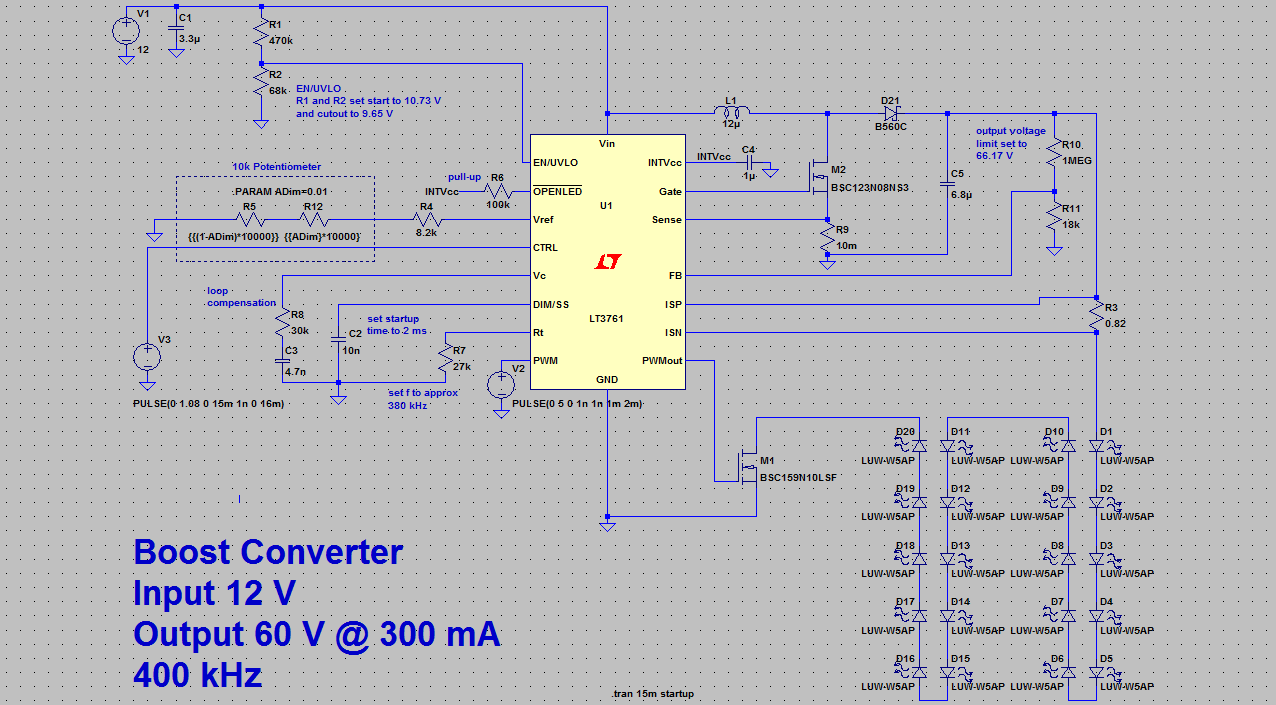
Continuing on from my recent post on designing a DC-DC converter for an LED panel, I've done a preliminary simulation of a boost converter using the Linear Technologies LT3761 to investigate some of this issues that need to be considered.

You can download the LTSpice file for this project from the Github repository.

This simulation is mainly to see if this kind of topology is feasible.  It allows me to choose components, see how much current they'll draw, and how much power they'll dissipate, if there's anything obviously wrong, I can make adjusts before I get too far down the track.

In the simulation below I haven't taken advantage of the features that allow the output current to be varied.  I wanted to keep it simple to start with.  The circuit is essentially a reference design from the datasheet that's been adapted for my specifications.  To simulate the LED panel, 20 LEDs have been connected in series.  It was previously verified in a different simulation that this arrangement of LEDs has a similar voltage-current curve to the panel I am trying to drive.

Electronic Schematic
Boost Converter Schematic
The converter seems to be doing its job, the current is around 300 mA and the voltage is around 60 V.  I'm concerned about the overshoot at start up, but it only lasts for around 400 us, which should be OK.  It's possible that I may be able to get better results by adjusting the compensation components connected to Vc, or changing the startup time capacitor on DIM/SS.

Graph of Electronic Simulation Results
Start Load Current and Voltage

I'm also concerned about the specifications for the inductor.  I need to make sure that the peak current is less than the saturation current.  I haven't looked into this yet.  If there's a problem it may mean I have to change topology or the operating frequency.

Graph of Electronic Simulation Results
Inductor Current

I took the opportunity to take some power measurements from the simulation as well.  The converter averages 18.718 W input while delivering 17.868 W to the load making it 95.4 % efficient.  Some other power readings are as follows.

Boost MOSFET - 454 mW
Inductor - 84 mW
Schottky Diode - 193mW
MOSFET sense resistor - 22 mW
Load sense resistor - 76 mW
LT3761 - 83 mW
PWM MOSFET - 1.05 mW

The numbers don't add up correctly (due to rounding and numerical simulations), but they at least give a ball park estimate of the power dissipation of components.

I know it's SPICE and the real world doesn't match the simulations, but I'd like to spend a little bit more time tweaking the design in SOFTWARE before I commit to anything.  That's a job for the coming week.

12 to 60 Volt 300 mA DC-DC Converter Design - Part 3

$
0
0
I've done a little more work on my design for a boost converter.  You can catch up on my previous posts here.

12 to 60 Volt 300 mA DC-DC Converter Design
12 to 60 Volt 300 mA DC-DC Converter Design - Part 2

It's been a busy week, so I haven't managed to get a lot done, but I've have made the design more stable and experimented with ways to dim the LEDs.  I've reduced the capacitor (C2) that controls the startup time from 20 to 10nF.


Electronic Schematic
Boost converter schematic.

The overshoot on startup seems to be a lot less now.  Startup time is still shown on the schematic as 2 ms but it's really 1 ms.

I've added two voltage sources that can control how the LED panel is dimmed.  It can be done by using a PWM method or by reducing the drive current of the panel.  First up I'll demonstrate the PWM method by driving the PWM pin with a square wave.

You can see that the initial pulse has a little bit of overshoot but after that it's a nice stable waveform.  The current though the LEDs is shown in dark blue.  Not shown in this plot is a current spike when the the load is switched back on.  It goes up to about 2.4A for a couple of micro seconds.  From what I can tell, this is due to the junction capacitance of the LEDs charging up and shouldn't be damaging.  I also think it's unlikely to happen in a real world circuit.  You can see the other side of this effect in the green line which is the voltage across the LEDs, after the load is turned off the junction capacitance starts to discharge.  As these are LEDs, even though there is still 40% ish of the operating voltage across them, there is essentially no current and no power, as indicated in the light blue plot.

Electronic Plot
PWM Dimming Waveform

Now on to the analog dimming mode.  This is controlled by applying a voltage to the CTRL pin.  The current through the load is equal to (Vctrl - 0.1) / (Rled * 4) for Vctrl under 1 volt.  Between 1 and 1.2 Volts this equation breaks down.  When Vctrl is 1.2 V the current supplied is at a maximum and the voltage across Rled is regulated to 250mV.  In my circuit this gives a maximum load current of 304 mA.

Just to test things out, I put a ramp voltage on the CTRL pin.  There is a bump at the start which I think has something to do with how the LT3761 regulates the supply, but I'm not sure.  Either way it doesn't matter, it's low down in the supply range of the LEDs

Electronic Plot
Analog Dimming Method

I don't intend to use this control method, but you can combine the analog and digital dimming methods as shown below.

Electronic Plot
PWM and Analog Dimming Method
To overcome the initial bump in the current waveform I tried delaying the ramp voiltage on the analog dimming method, but it didn't seem to have much effect.

Electronic Plot
Delayed Ramp Voltage

Once again the thing I am concerned about is the current in the inductor shown in purple below.  The steady state current doesn't worry me, the peak current on start up is way too high though.  I don't want to buy an inductor that's 3 times the size I need only to handle startup current.  I've been playing with the simulation and I think that I can control this by controlling the voltage on the CTRL pin more carefully on startup.  Essentially it needs to be ramped up slowly.  Hopefully I can have this sorted by my next post, have some actual components selected, and look at laying out a PCB.

Electronic Plot
Inductor Current


As usual, you can find files associated with this project on the Github repository.

How Can Current Flow Backwards Through The Inductor of a Boost Converter?

$
0
0
I've been keeping myself occupied by (slowly) designing a boost converter for an LED light panel, and during one of my simulations I noticed something weird, there was current flowing backwards through the inductor.  I couldn't seem to find any reference to this anywhere so I thought I'd write up what I think is happening.

First I'll give a quick explanation of how a boost converter is meant to work using the schematic below.  When the power mosfet M2 conducts, the input voltage is placed across the inductor L causing the current through it to rise.  When M2 is switched off, the current through the inductor now flows through D21 to fill the capacitor C5 and supply the load.  I won't go into the maths, but it's trivial to calculate the voltage gain of the converter.  It's important to note that current can't flow backwards through the inductor at any point.  For this to happen, current has to either go backwards though the diode D21 (which happens a tiny bit, but isn't what we're seeing) or it has to come out of the mosfet M2, which doesn't make much sense either.

Schematic
Boost converter schematic
The simulation that initially caused me to look into this is below.  It occurs during startup, when the output capacitor isn't fully charged and when the controller is in soft start mode.  At this point the circuit is operating in discontinuous mode, meaning that the inductor current will fall to zero during each switching cycle.  Nearly every textbook will illustrate this with a triangular waveform with a flat section in between triangles to indicate the zero current section.  This isn't what happens though.  I'll step through the stages of operation in the image below.

  1. The mosfet is turned on (gate voltage is the green waveform) and the current in the inductor starts to ramp up (light blue).  The voltage at the point between the inductor and mosfet drops to zero (red) and there isn't any current flowing through the diode (dark blue).
  2. The mosfet is turned off.  The current flowing through the inductor starts to ramp down.  The voltage at the point between the inductor and mosfet increases to near the output voltage. It can be seen that the inductor current goes through the diode as the dark and light blue plots are the same in this section.
  3. This is the point where traditional explanations fail.  The mosfet is still off and the diode current has reached zero.  The voltage between the mosfet and inductor starts to fall as you would expect.
  4. The inductor current keeps ramping down though, and in this case reaches around 200 mA in the reverse direction.  The only place this can come from is the mosfet.

electrical waveform
Boost Converter Simulation
So what's going on here?  I contend that this can be explained by taking the parasitic capacitance of the mosfet and diode into account.  I'll leave exactly what capacitance causes this up to someone more familiar with semiconductor physics.  To demonstrate this and remove other variables I've put together a simplified model below.

The input voltage source remains. As the output capacitor is made increasingly large it starts to act like a voltage source, therefore it can be replaced with a voltage source set to the output voltage we are interested in, and a steady state analysis can be performed.  The mosfet has been replaced by a voltage controlled switch with a parallel capacitance, in this case 500 pF, to represent the parasitic capacitance.  A reverse biased diode has also been placed in parallel to represent the mosfet body diode.  The Schottky diode connected to the output has been replaced with an ideal diode with an appropriate forward voltage.

Electrical Schematic
Simplified Model
Note: I apologise for the graphs, you may need to click on them to see things more clearly.  The voltage and current scales don't have a common zero either.

Running this simulation gives an almost identical plot to the one above, but we can now see what is happening more clearly.  The inductor ramps up as before (dark blue), it then ramps down to zero amps and the output diode stops conducting (red), but we can now see that the parasitic capacitance is still charged (green), it starts to discharge, but can only do this via the input inductor.  This is the reverse current through the inductor.  What's happening is that the parasitic capacitance is resonating with the main inductor around the zero volt point.  In the simulation below the resonance occurs at a frequency that makes it look like it's part of normal operation.  The period of resonance for an LC circuit is 2*pi*sqrt(LC), in this case that's equal to approximately 0.5 us.

It's hard to see but you may also notice a tiny delay between the time the mosfet is turned off and when the diode starts to conduct.  This is the first bit of current from the inductor charging the parasitic capacitance.  Once this capacitance is charged and the voltage reaches a high enough point, the diode will then start to conduct.

electrical waveform
Simplified simulation
All of this can be made clearer by shortening the on period as seen below.  Ideally the time spent with a negative inductor current should be around half a period of the resonance 0.25 us, which is close, but there is another effect at play that can be see in the green trace.  The voltage between the inductor and mosfet hits a limit of -0.7 volts.  At this point the body diode starts to conduct, effectively dampening the resonance.

electrical waveform
Simplified simulation - reduced on time
If we were to reduce the parasitic capacitance by a factor of 5, the resonance period would be reduced by a factor of sqrt(5), giving 0.22 us.  Which is once again close to the simulation below.  This time the resonance is clearly seen in the voltage between the inductor and mosfet.  It can also be seen where the bottom of a typical resonance waveform has been clamped by the body diode.

electrical waveform
Simplified simulation - lower capacitance
This is another one of those theoretical cases.  I don't know if this will really happen when a real device is built.  I don't even really know if it's a bad thing, I just had to put an explanation up in case someone else has the same issue.

You can get the related files here.

Edit:  On reflection, it is a bad thing.  High frequency noise is a bad thing in any circuit and leads to EMI problems.  I've since found out that googling "Boost Converter Switch Ringing" will yield more information about this issue.

Boost Converter Startup

$
0
0
My ongoing series on designing a boost converter continues.  Today's post will be short one.  What happens in the converter during startup?  The period between when you first apply power and when the controller starts to do it's thing.

Using the schematic further down the page as a reference, the startup waveforms below can be described.  It's also helpful to know the period of an LC oscillator as well.

equation
steady state period of an LC oscillator
  1. During startup the power mosfet (M2) is off, and can be ignored in this analysis.  The current in inductor L1 (36 uH) is zero and the voltage across the output capacitor bank C5, C7, C8, C9 (9.9 uF) is equal to zero.  When the 12 volt supply is first applied, the inductor L1 and the capacitor bank start to resonate.  This causes the initial peak.  The initial inductor current (purple) should resonate around zero amps.  Knowing that the peak voltage deviation will be 12 volts (i.e. the voltage across the capacitor will have a range of 12 ± 12 volts) it can be shown that the current through the inductor L1 will be equal to 12*sqrt(C/L).  In this case that equals 6.29 Amps.  We get close with around 5.8 Amps.  The forward voltage of the diode means that the supply is more like 11.4 Volts and there are also some series resistances that will cause the current to be lower.  That equation is only valid for steady state analysis as well.
  2. In theory the voltage across the capacitor bank (red) should peak at double the input voltage, as an undamped LC circuit will swing to double the magnitude of a step input to give 24 Volts.  In this case however, the forward voltage of the diode and small resistance of the inductor has reduced this to the 22.4 ish volts observed in the simulation.  At this point we have approximately one half period of oscillation.  Although meant for a steady state conditions, this can be checked against the formula above.  t = 2*pi*sqrt(LC) = 118us.  Half a period is approximately 60 us, pretty close.  Another effect starts to happen at this point as well, for the first time the inductor current goes to zero and tries to reverse.  The diode doesn't allow this to happen, leaving the output capacitors charged at around 22.4 volts.  The inductor starts to immediately resonate with the parasitic capacitance of the mosfet.
  3. The damped oscillations have a period of approximately 1.05 us.  Using the equation above it can be shown that the parasitic capacitance is 775 pF.
  4. The current ripple can also be seen in the inductor.
(Click for larger images)
electrical waveforms
Startup waveforms of a boost converter


Boost converter schematic
Boost converter
Get the associated files here.


Boost Converter Output Capacitor Selection

$
0
0
I was a day late with this post as I was trying to select capacitors for my boost converter.  I knew it wouldn't be easy, but I didn't think It would be this hard.  The loose specification I'm trying to achieve is listed in this post, but basically I'm trying to convert 12 to 60 Volts driving a 300 mA load.

I started by looking at different converter topologies, and decided to go with a boost converter due to what parts I could get (I didn't want to hand wind transformers - walk before I can run).  I'm reasonably sure it's not the optimum topology, but it should be doable with off the shelf parts.  I'm at the point where I've got a stable design that does what I want, and am now trawling through suppliers to find actual parts.  Things were going great,  got an inductor, got a switching Mosfet, got a Schottky diode, hit a wall when it came to the output capacitor.

The problem is that the capacitor needs to be rated for 60 Volts, and to minimise ripple needs to be low ESR, and has to be around 5 uF.  That's like trying to find pixie dust.  Let's look at the equations that determine what capacitor I'm looking for and see if we can't tweak some things, keeping in mind that the purpose of the output capacitor is to minimise ripple in the output voltage.

Equation
Levels of Output Voltage Ripple in a Boost Converter

The output voltage ripple consists of two parts, the first part occurs when the capacitor discharges while suppling the load while the Mosfet is on and charging the inductor.  This means it's related to the duty cycle, frequency of operation, load current and the capacitor size.  I can't change the load current or the duty cycle, but I did decide to up the frequency of operation from 400 kHz to 600 kHz.  This means I can get away with a smaller capacitor.

The second part of the voltage ripple is caused by the ESR of the capacitor. When current flows into and out of the capacitor through the ESR during its charge discharge cycle, a ripple is created.  Reducing this ripple can be done in two ways, decrease the ripple current in the inductor, or get a low ESR capacitor.  I've increased the inductor size to reduce it's current ripple, but the best option is to select a low ESR capacitor.  Ceramic capacitors have such a low ESR they are essentially considered to have none, and for this reason have become a favourite in DC-DC converter designs.  When going through all my searches and considering specs against cost, they're pretyy much the best option.  They have one drawback though, when biased with a DC voltage their capacitance is reduced.  In some cases, significantly.  I'll let EEVblog explain.


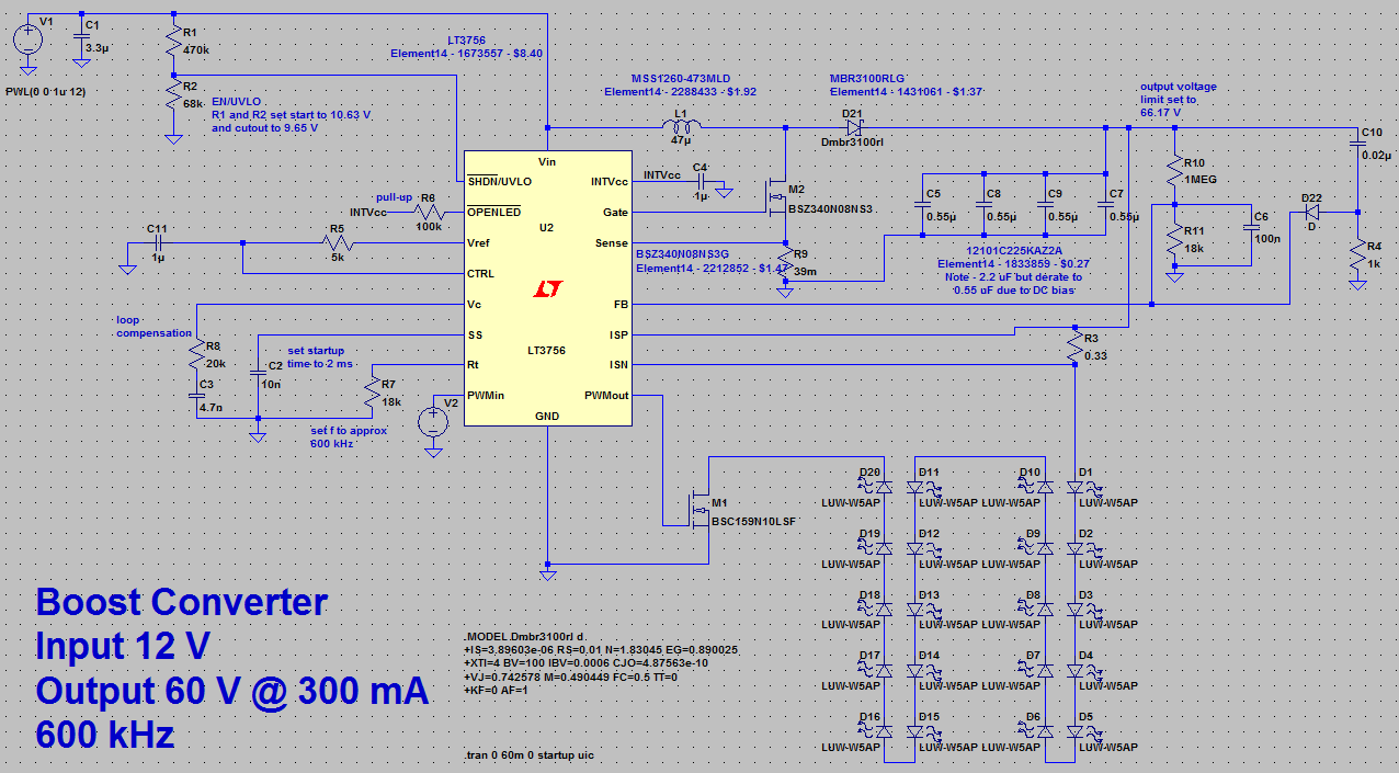
So finding the capacitance I need isn't easy, particularly when I need to find parts rated to 60 Volts.  In the end I decided to go with 4 x 12101C225KAZ2A from AVX.  They're X7R 2.2 uF capacitors rated to 100 V each and when biased to 60 V I should get at least 550nF out of them, giving a total of 2.2 uF.

I need to investigate how the dynamic resistance of the load interacts with all of this, but in the end I think everything should work.  I've upped the frequency of operation, and slightly compromised on my acceptable level of ripple.  After all, isn't engineering is the art of intelligent compromise?

Electrical Schematic
Boost Converter Design

.

LED Driver Boost Converter

$
0
0
So, it's time for an update on the LED driver I'm designing.  I think I have the final design of the circuit and have most of the components selected.  I haven't bothered selecting actual parts for non critical components yet.  The design is mostly locked in, a value may change here or there but it's pretty much final.  The input filter added to remove conducted EMI may need some improvement as there may be the possibility of ringing.

I'll admit that this has taken longer than I would have liked, but I took it as an opportunity to learn how all the components of a boost converter interact and change the overall operation.  I didn't want to blindly follow a reference design and not know what I was doing.  I still have a lot to learn, particularly about compensation and stability, but it's been fun.

Boost Converter LED Driver - with PWM and Analog Dimming

The plot below shows the circuit starting up.  The PWM dimming function is in use with the frequency being swept from 0 to 3kHz.  The output slew rate limiting circuit does its job and brings the output voltage up gradually without causing too much current to flow through the main inductor.

LED Driver Sweeping the PWM Frequency from 0 to 3 kHz over 60 ms

In the plot below you can see a cycle of the converter operating.  The LED currentin dark blue slightly overshoots its target but comes into regulation rather quickly.  The main inductor current is shown in light purple and can be seen to have ripple, but nothing that wasn't anticipated.  The main supply current is shown in dark purple and has no noticeable high frequency component, but there is some ringing,  I don't want that.  So this area needs some attention.  If anyone has experience with this I'd be glad to take suggestions.

I've simulated the snot out of this thing, but that can only get you so far.  So it's time to actually do a board and see what happens.

Main Inductor Current, Supply Current and LED Current

You can grab the associated files from the GitHub Repository

MeanWell LDH-45A-350W Dimmable LED Driver Evaluation

$
0
0
As you may have seen I've been designing a DC DC constant current power supply to drive some LEDs from a 12 Volt supply.  The main reason for doing it myself was because most of the drivers I've seen don't have a feature to dim the LEDs by reducing the drive current, they typically drive the LEDs at full power and pulse them on and off to vary the brightness.  This can be an issue when used for photography.

I'm getting there slowly, and am close to laying out a PCB, but during my research on LED drivers I found a nice little unit from Mean Well power supplies that allows you to dim LEDs by PWM and Analogue dimming.  Granted, they have one of the least reassuring names in the electronics industry, but I like their stuff and have never had an issue with them. (I think I've used their products 4 times before)  So I thought I'd get one and see how a professionally designed unit performs.  They're cheap enough, you can get one like mine for $20 excluding postage.

LED Driver
MeanWell LDH-45A-350W LED Driver

As the unit is potted I can't do much of a teardown, but I did pop the back off and you can see some of the signs of a switch-mode converter.  In two locations you can see arrays of vias probably used to dissipate heat into the copper pour from switching elements like diodes or transistors, and small traces coming off large areas most likely indicate parts of the feedback circuit.


LED Driver PCB
Bottom side of LED driver PCB

The banner specs are also worth a look.  The datasheet is for a family of converters, I have the 350 mA model.  I'm happy that they comply to an EMI standard, most cheap stuff from China doesn't worry too much about things like that.  Short circuit protection is expected, there's most likely a transistor on the low side of the LED string that's used for PWM control, when an over current is detected this transistor simply shuts off disconnecting the load.  Encapsulation is good as well, the unit feels rugged, like it would take some abuse.

Electrical Specifications
LDH-45 LED Driver Family Specs

My unit is capable of outputting up to 86 Volts and my panels run at 60 Volts, so that's fine.  The voltage input range is also fine, although there is a derating curve in the datasheet.  Any Vin lower than 12 Volts won't be able to drive the LEDs at full current.

Electrical Specifications
LDH-45A-350 specs

Usage is fairly straight forward, the input voltage is connected to the Vin+ and Vin- wires and the LEDs are connected to the Vout+ and Vout- ones.  That's all you need to do if you dan't want to use the dimming features at all, but it will drive the load at full capacity, 350 mA, and my panel is rated for 300mA, so I need to reduce the drive current.  For this post I'm not using PWM dimming, I'm just focussing on analogue dimming.

Reducing the drive current is as simple as placing a control voltage across the Analogue DIM and DIM- wires.  I assembled a test rig as per the diagram below using an adjustable power supply.  The LED panel I used to test the driver was the one I recently did a review of.  Voltages and current were measured at various places around the circuit.  You can get my measurements and the datasheet from here.
Electrical Circuit
Test setup

First up I wanted to check the relationship between the analog dimming voltage and the output current.  The datasheet gives a graph for this.  It's basically a linear relationship between 0.25 to 1.2 Volts.
Electrical Graph
Analogue dimming voltage control from the datasheet

Remarkably, my results were pretty much spot on.  I couldn't go to 100% drive current, but the curve matches well for the tests I performed.
Electrical Graph
Measured analogue dimming voltage control

I then wanted to test the efficiency of the unit.  The datasheet has a graph, presumably at full current, for the maximum efficiency of different number of LEDs with a Vf of 3.15 Volts.  In my case that would be 19 LEDs for an efficiency of 0.932
Efficiency
Efficiency for different LED configurations

Once again my measurements compared well. Once a decent load was applied I was able to get a consistent efficiency of around 92 percent.  Not too shabby at all.  This is great, due to its efficiency, it doesn't get noticeably hot, which means no active cooling needed. (YMMV depending on how enclosed it is)
Electrical graph
Measured Efficiency for different load currents

For my own reference I wanted to do some electrical tests.  These are all performed with an output current of 300 mA

I wanted to see how noisy the converter was electrically and its operating frequency.  The first test I did was to clip the ground lead to the probe tip and hold it over the device, a poor man's EMI probe if you will.  You can notice that the device appears to be running at 95 kHz.  This is surprising as my design runs at close to 600 kHz, mine could be smaller, but may have more loss.  You can also see a few spikes created by switching elements.  I could guess what they are, but as I don't know the exact topology used I'd only be guessing.

Electrical Waveform
Scope probe loop held over the converter

I then check the input voltage ripple of the power supply, it's in the 50mV range.
Electrical Waveform
Input voltage ripple


I then checked the input current.  As I didn't have anything specifically set up to do this I clipped the probe leads across the input to a multimeter and used the internal shunt to measure the current.  Quick and dirty.

You can see that the input current resembles the charge discharge cycle you'd expect from a boost converter.

Electrical Waveform
Input current

As the input current is about 1.67 Amps, the ripple is around 30 mA.
Electrical Waveform
Input current ripple

There is also a bit of ringing in the input current, that could be the EMI filter or just inductance from all the test leads I was using.
Electrical Waveform
Input current ringing

I measured the output current in a similar way.  It was measure to be 300 mA by multimeter.
Electrical Waveform
Output current

The spikes in the output current have a magnitude of about 180 mA. Once again, this type of thing may be due to the way I'm measuring things.
Electrical Waveform
Output current ripple

You can see ringing in this case as well.  L and C as far as the eye can see.
Electrical Waveform
Output current ringing

Nothing too exciting here, the output voltage is 60 Volts.
Electrical Waveform
Output Voltage

Ripple in the output voltage that looks like this could be down to the ESR of the capacitors in the output filter.  As current flows into them, V=IR causes the voltage to rasise slightly, when they discharge the voltage drops.  Just speculation, but at 60 Volts, what's a couple hundred milliVolts between friends.
Electrical Waveform
Output Voltage ripple

I was very interested in the startup profile as I had a hard time getting mine to behave.  From the the point the voltage starts to rise it takes about 25 ms to get to the a stable output voltage.  There doesn't appear to be any noticable overshoot.  All in all quite nice.

Electrical Waveform
Startup voltage waveform
I'm definitely going to use these again.  They have all the features I want and are simple to use.  I'll need to come up with something to control the dimming inputs, but that shouldn't be too hard.  If they're using a chip similar to what I've been using in my design, you should also be able to use the analogue and PWM controls at the same time.

I really didn't want to build multiple units like this, don't get me wrong, I want to learn how to do it, but it's hard to beat a self contained module that sells for $20.

Three Terminal Resistive Network Conversions

$
0
0
Warning - This article describes equipment and circuits that operate at high voltages.  Don't attempt to repair any high voltage circuits if you're not trained to safely work with electricity.  You may be seriously injured or even killed.  For further information read the blogs Terms Of Use. 

Recently I solved an electrical problem that got me thinking about 3 terminal networks, so I thought it would be a great opportunity to explaining how to measure and convert between the different topologies.

The Problem

I got a panicked call from my parents recently after they'd lost power and were unable to turn it back on.  I did the basic things before getting there, like checking the website of the power company for any outages, then checking twitter for any car accidents in the local area that could have cut power by damaging a power pole, but I drew a blank.  On a arrival the problem became clearer, they could turn the power back on, but five minutes later the residual current device (RCD) would cut out.  This indicates that an appliance had a fault, but not so serious that it would immediately trip the breaker.

To isolate the problem, all the individual circuits were turned off, then turned back on one at a time, waiting 5 minutes between each one.  The next step was to find the appliance on this circuit, the same process was followed, all the power points were turned off, and then gradually turned back on until the problem was found.  It turned out to be my mothers laptop power supply.

Power Supply
Toshiba Laptop Power Supply

I assumed that something like a capacitor in the input filtering circuit had failed, or the transformer had failed somehow, either way I'd accepted that the supply was dead.  I thought it'd be interesting though to find out how damaged it was.  To test this, I set up a test power point with it's own lead, but didn't connect the Earth.  On the back of the power point I connected a multimeter between the Earth and Neutral terminals.  This allowed leakage current to flow through the ammeter to neutral, without causing the main RCD to trip.  This was all powered by an extension lead that I could turn on and off from a safe distance. (I HATE mains voltage)  Also make sure that there are no children or pets around that can distract you or get injured.  The power point was dissembled and made safe immediately after the test, leaving dangerous things that look safe laying around is asking for trouble.

Power Supply
Toshiba Laptop Power Supply

I started the test and measured a small leakage current of 6 mA, but also heard a small crackling sound.  I shut everything down and did an inspection of the power supply.  The C5 type input plug was noticeably hot.  At first it kind of made sense that the hot spot was near the entrance to the power supply, that's where all the mains components should be, but the plug was way hotter than the power supply.

Electrical Plug
C5 Laptop Connector

On closer inspection I noticed what looked like melted plastic on the plug itself.  It could be left over from manufacturing, but the other side looked fine.  With the plug removed, I measured the resistance between all three prongs on the mains plug and got results in the range of 30 to 70 kilo-ohms.  When the lead was tested by itself with mains power and no load, the lead still got hot.  That shouldn't be.

Electrical Plug
Burn Marks on C5 Laptop Connector

To wrap things up I replaced the lead with an old one and have had it plugged in for about 5 hours now with no problems.  I don't know how the fault occurred, it seems strange to have resistance between all three pins.  It seems like something that a liquid spill could cause.  Other than that, I don't know.  After writing that last sentence I went and checked the resistance on the outside of the plug, I picked two random points and got around a mega ohm.  The outside shouldn't be conductive at all, so I'm almost certain that something was spilled on it, even if it wasn't noticed when it happened.

Three Terminal Resistive Networks

All the talk of resistance between 3 terminals got me thinking about delta and y topologies.  In the diagram below you can see the C1332 style Australian mains power plug.  The discussion above describes measuring the resistance between all three pins, but how would you represent that in a circuit if you wanted to model it?  You can't simply place resistors equal to your measurements between the pins in a triangle arrangement.  Measuring between Earth and Neutral would then give you that resistance in parallel with the sum of the resistance between Earth and Active, and Neutral and Active.  So we need to do some maths. Yayyyyyy!!!!

Electrical Plug
Australian C3112 Style Mains Plug

I find it easiest to start with what's called the Y or wye configuration.  It's called that because you place three resistors in a Y shape, as seen below.  You have a similar problem though.  Measuring between any two terminals gives you the sum of two resistors,  for example measuring between Active and Neutral gives the sum of the resistances R1 and R2.  It's trivial to write three equations to describe this arrangement and then solve the simultaneous equations.  I've done it via the reduced row echelon method.  You can now use the values of R1, R2, and R3 to model the circuit.

You can also model the circuit using a delta arrangement, which is three resistors in a triangle between the terminals.  Converting between the Wye and Delta topologies is easy enough and is a well known conversion.  After performing the conversion you can use the resistors Ra, Rb, and Rc in a delta (triangle) arrangement to replicate the circuit.

Engineering Calculations
Delta-Wye Calculations

Another technique not as well known uses an iterative method to go straight from measurements to the delta resistor values.  You write out three equations that describe your circuit and the values you want to find, make estimates for all three values, in this case 50 kilo-ohms was a good starting point.  You then use one equation and two variables to calculate a new guess for the third variable.  Do this for each variable and repeat until the resistor values converge. I've used a different naming convention in the example below (my bad), but you can see the process in action. The first equation uses guesses for Ry and Rz to calculate a new value for Rx, the second equation uses Rx and Rz to calculate a new value for Ry, and the third equation uses guesses for Rx and Ry to calculate a new value for Rz.  This is repeated until the values converge.

This is a numerical approach that sometimes works, it depends on how well behaved the equations are and if they converge.  For example if you were to use this method to get from the initial measurements to the Y configuration it would fail and the resistor values wouldn't converge, they'd just oscillate.  Typically you need a division by one of the variables in the equations for it to work.  I'm sure there's a formal mathematical definition for when it will and won't work, but I'll leave that for someone with more time, sleep, and mathematical ability.


Spreadsheet
Iterative Spreadsheet Solver


The above spreadsheet can be found here.

Using a Raspberry Pi to Log Songs Played on a Radio Station

$
0
0
I recently came up with an idea that required me to build a device to log the songs played on a radio station.  There are a few ways to go about this, you could scrape the data from their streaming radio service, you could use something like Shazam to identify the songs and record them, or you could use the RDS data encoded in the radio signal.  I decided to go the RDS way.

Nearly everyone is familiar with the RDS data stream even if they don't know it.  Newer car stereos that display the current song playing get this from the RDS data.  The FM radio station is first demodulated.  In this demodulated signal at 57 kHz there is double side-band suppressed carrier that contains the RDS data.

The initial method I chose to receive this signal didn't work.  I planned to use a software defined radio approach using an RTL-SDR dongle and a Raspberry Pi, but I just couldn't get it to work.  After some Googling I came up with Plan B.  Use an FM radio receiver IC that contained an RDS decoder and connect that to a Raspberry Pi.  Luckily, Sparkfun had a breakout board for the si470x that was perfect for the job.

I didn't want this to be a massive project so I grabbed publicly available code and modified it for my purposes.  The code was tested until it could run for long periods without crashing.  There's no exception handling, I just reduced the errors until the system was stable.  I could have spent another couple days making it "perfect", but what's the point, this isn't a product or a permanent installation, it has to run for a week or so and give me usable data, and it's doing that.  Currently at around 45 hours.

The code for this project is available from github.  I urge you to have a read of the README file there it contains more information about the code.


Based on code from


RDS receiver and logger
Raspberry Pi and si470x based RDS receiver/logger
The system above looks complicated, but it really isn't.  The white brick in the lower left is a USB power supply.  The Raspberry Pi is the device at the top left, connected to it by jumper wires is the si470x breakout board.  The Pi is also connected to a USB 3 hub that has a Wi-Fi dongle and a USB 2 hub connected to it.  That may sound strange, but the Pi can't recognise USB 1.1 devices plugged into a USB 3 hub, so you need a USB 2 hub in there to allow the connection of the mouse and keyboard.  Yeah, I could have done this via an SSH terminal, but as I was connecting wires directly to the Pi it just seemed easier to be at the device while I did it.

The software is simple as well.  I modified the original code to just constantly poll the si470x receiver, log the RDS messages with timestamps and station frequency, and then rotate the logs hourly.  The script was also configured to run as a background service on start-up.  So if it loses power, it should just automatically start logging again.

I also planned to run the dropbox_uploader utility on a schedule with a cron job to backup the log files.  I wrote the script to do this, but it seemed easy enough to run it manually every now and then.

Log file
RDS log file
The RF signal chain is important, you need a good signal to get the RDS data.  Even if you can hear the station clearly you still might not be able to receive song names.  The si470x breakout board uses the headphone wiring as the FM radio antenna, just like most phones, if you want the radio to work you have to use some type of headphone.  The presence on a human body also boosts the signal.  This is a nice solution in most cases, but I couldn't sit there wearing headphones for a week.  Well, I could but I don't think I'd have a job at the end of the project.  I guess that'd be a bad thing, maybe.

To get a good signal I took a folded dipole antenna made of ribbon cable I just happened to have and used that, I put it on a table and put some books on the end to stop it rolling up.

Antenna
300 ohm Folded dipole ribbon cable antenna
The folded dipole has a 300 ohm balanced output, but I needed a 75 ohm unbalanced signal, so the antenna was connected to a balun.

Balun
300 - 75 Ohm Balun
To get the coax signal into the breakout board I used a simple adapter.  In terms of impedance matching it's not ideal, but I did the best I could with the rest of the chain so it turned out OK.

coax to 3.5 mm adapter
Coax to 3.5mm plug
Connecting the Raspberry Pi to the si470x breakout board is relatively easy, just be careful GPIO 23 is actually pin 16, don't know who came up with that idea.
Connection Diagram
Add caption
I had a lot of fun with this project. It took a week of coding and fiddling in my spare time to get it working.  I'm pretty happy with that.  I'm usually more self concious about my coding ability, but you know what, fuck it.  I made something that does what I want, and if anyone has issues with my code they're more than welcome to improve it and do whatever they want with it.  I'd love that.  That's why it's out there, to help the next person that comes along.
Viewing all 99 articles
Browse latest View live